
Reliability in Printed Circuit Board Assemblies
When it comes to printed circuit board assembly (PCBA), reliability isn’t just a goal, it’s an imperative. Without proper reliability testing and assessment, the integrity of a PCB is in jeopardy and could ultimately render a finished product useless. In fact, many commercial products are required to pass a series of tests that go far beyond the functional testing performed on most electronic devices. These reliability tests are essential to weed out early failures and ensure that the devices perform as intended in the field.
During the manufacturing process, a PCB can be subjected to mechanical, thermal, and electrical stress. All of these can degrade the quality of a device and cause premature failure. This is why stress testing analysis is critical to ensuring the quality of a completed electronic product.
Mechanical stress can cause physical damage to a printed circuit board assemblies by creating stresses on the copper foils and solder joints. These can lead to the deterioration of surface routes, signal layers, and ground planes and result in poor functionality or even a complete failure. Conducting a stress test can help to identify these issues during the design phase and make necessary adjustments to protect against them.
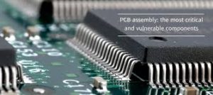
How to Ensure Reliability in Printed Circuit Board Assemblies
Thermal stress can be caused by cycling between extreme temperatures, poor heat distribution, or stacking too many buried vias. Poor thermal management can also create hotspots that can physically damage components over time. The stress induced by these issues can be mitigated through proper layout and component selection.
The PCB’s layer stack-up is vital to signal and power integrity, as it determines the dielectric constant of the materials used. These properties influence the transmission of signals across the board, and require careful selection when developing a high-reliability product for harsh environments.
The electrical stress of a PCB can occur through a variety of causes, such as shorts, capacitance mismatches, and ionic contamination. This can be mitigated through a variety of techniques, including a burn-in test and environmental stress screening (ESS) to weed out early failures and identify potential issues before they become problematic.
During the ESS, a sample of PCBAs are subjected to various environmental conditions to replicate field deployment and identify possible failure modes. This can include accelerated aging and thermal cycling to measure the stability of a product under environmental stress. Using a stress test can help to identify these failure modes during the design phase and make appropriate modifications before production.
When selecting a manufacturer for PCB production, be sure to ask about their sourcing procedures and QA programs. A robust supplier network helps reduce the risk of supply chain issues, such as component shortages or delays, that can impact the quality of a product. It’s also important to look for a manufacturer with a strong track record and industry experience in order to verify their ability to produce reliable boards.


