
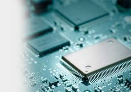
High Density Interconnect PCBs
High-density interconnect pcbs are printed circuit boards that use microvias and printed through holes (PTH) to facilitate vertical interconnections. This technology enables the production of thinner, lighter, and more complex devices with a higher performance and reliability. It is used in a variety of industries, including aerospace, military, and medical devices. It has a number of benefits over traditional PCBs, including improved thermal management, faster signal transmission, and reduced power consumption.
high density interconnect pcb offer many benefits, including reduced manufacturing costs and improved signal transmission and efficiency. They also offer better thermal management, allowing heat to escape more easily, which can reduce stress on the components and extend their lifespan. They also offer greater design flexibility, allowing engineers to optimize circuit layouts and minimize trace lengths. They are also able to accommodate smaller BGA and QFP packages, which can be difficult to fit on conventional PCBs.
The advantage of HDI circuit board construction is that it allows you to create a more compact device, which can help you save on materials and space. This is particularly important in the case of handheld devices and equipment, where size and weight are vital factors.
Advantages of High Density Interconnect PCBs
Another benefit of HDI circuit boards is that they have a lower temperature than standard PCBs. This is because they have shorter paths for heat to travel, which can help to avoid overheating. This can lead to longer battery life in your device. In addition, the reduced power usage of HDI circuit boards can help to reduce your environmental impact and cut down on waste.
HDI PCBs also have improved signal transmission, thanks to the smaller trace widths and tighter spacing. This can allow for more components to be packed into a small area, and can lead to significant reductions in signal loss and crossing delays. This technology is also used in a variety of different applications, such as consumer electronics, aerospace, and automotive vehicles. It is particularly useful in the healthcare field, as it can help to make medical equipment and devices much smaller and more portable.
How does the manufacturing process of a HDI PCB work? The process begins with photoresist deposition and exposure. The exposed photoresist is then etched using the current industry standard etchant, which is ferric chloride. The remaining photoresist is then buffed off and the resulting conductor pattern is metallized. The layers are then stacked in multiple lamination cycles before outer layer processing.
In the case of 2+N+2 HDI, the inner signal layers sandwich two outer power layers. This can reduce reworking and assembly issues and improve reliability. It can also reduce component heights, which makes the board more compact and efficient.
The best way to get the most out of your HDI PCB is to find a supplier that offers quick turnaround times and high-quality products. This will ensure that your project is completed on time, and will help to increase cost-effectiveness. Choose a company that has extensive experience working with this type of product, and that can provide you with the right solution for your needs.

