
create a PCB prototype
Creating a PCB prototype is an essential part of developing an electronic device, allowing designers and engineers to test and validate their circuit designs before moving to mass production. The process involves multiple stages, from initial design to fabrication, testing, and refinement. In this article, we’ll explore how to create a PCB prototype, breaking down each step involved in its creation.
The first step in creating a PCB prototype is designing the circuit. This is done using PCB design software such as Eagle, KiCad, or Altium Designer. Engineers start by creating a schematic diagram, which outlines the components to be used and their connections. Once the schematic is complete, the designer then moves on to the layout phase, where the actual physical design of the PCB is created. This includes determining the size of the board, the placement of components, the routing of the electrical traces, and the inclusion of features like vias and solder pads. The goal is to ensure that the board functions correctly, fits within the desired dimensions, and can be manufactured without issues.
After the design is finalized, the next step in creating a pcb prototype is generating the Gerber files. Gerber files are the industry standard for PCB manufacturing and contain all the information needed to fabricate the board, such as copper traces, drill holes, solder mask layers, and silkscreen layers. These files are exported from the design software and sent to a PCB manufacturer for production. Ensuring that these files are accurate is critical, as any errors could result in a faulty prototype.
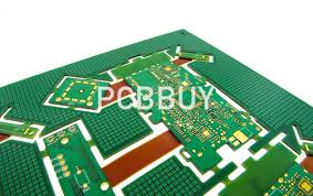
How do you create a PCB prototype?
Once the Gerber files are ready, the PCB prototype is sent for fabrication. PCB manufacturers use various methods to produce the prototype, including traditional methods like etching or more advanced techniques such as laser direct imaging. The manufacturer takes the Gerber files and uses them to create a physical board by applying copper layers to a substrate and then etching away the excess material to leave behind the electrical traces. Vias, which are small holes that connect different layers of the PCB, are also drilled at this stage. The board is then coated with a solder mask to protect the traces and prevent short circuits, followed by a silkscreen layer to print component labels and other markings.
Once the PCB prototype is fabricated, the next step is assembly. During this stage, components such as resistors, capacitors, chips, and connectors are placed onto the PCB. This can be done manually for small runs, but for larger batches, automated processes like surface mount technology (SMT) or through-hole technology (THT) are used. The components are soldered to the board, either using a reflow oven for SMT or wave soldering for THT. For complex prototypes, manual inspection and hand soldering may be required to ensure correct placement and soldering of components.
After assembly, the PCB prototype undergoes rigorous testing. This includes electrical testing to verify that the circuit works as expected. Engineers check for power integrity, signal routing, and any shorts or open circuits that may have occurred during manufacturing. Additional tests may include thermal testing to ensure that the components do not overheat, and mechanical testing to verify that the board can withstand stress and vibrations. If any issues are found during testing, the design is adjusted, and a new PCB prototype may be produced to address the problem.
Finally, after testing and refining the PCB prototype, the design can be optimized for mass production. Any changes made during the prototyping phase are incorporated into the final design to ensure that the PCB meets the desired performance, reliability, and cost targets. This iterative process helps minimize risks and ensures the final product will meet quality standards.
In conclusion, creating a PCB prototype involves a series of steps, from design and fabrication to assembly and testing. Each phase is critical to ensuring the functionality, manufacturability, and reliability of the final PCB. By carefully testing and refining the prototype, engineers can avoid costly mistakes in mass production and bring their electronic designs to life with greater confidence.


